Packard Bell 870 M/Board
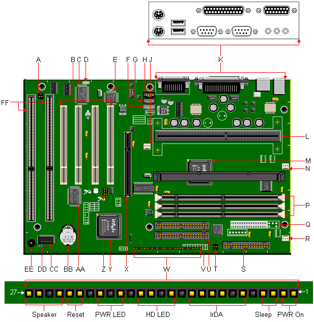
| Item | Description | Item | Description |
|---|
| A | Wake On Ring Connector | R | Fan 1 Connector |
| B | PCI Slots | S | Floppy Connector |
| C | SMC FDC37C777 Super I/O Controller | T | Front Panel Connectors (J8G2) |
| D | Wake On LAN Connector (Optional) | U | Secondary IDE Connector |
| E | Crystal CS4236B | V | Primary IDE Connector |
| F | Aux. Line-In Connector (Optional) | W | Front Panel Connectors |
| G | Telephony Connector (Optional) | X | AGP Port |
| H | CD-ROM Audio Connector (Optional) | Y | 82371EB PIIX4E |
| J | Fan 3 Connector | Z | PC/PCI Connector |
| K | Rear Port Connectors | AA | Crystal CS4611 PCI Audio Accelerator (Optional) |
| L | SLOT1 SEC Cartridge Connector | BB | Battery |
| M | 82443BX PCI AGP Controller (PAC) | CC | Flash BIOS |
| N | Fan 2 Connector | DD | System Configuration Jumper Block (J8A1) |
| P | DIMM sockets | EE | Piezo Speaker |
| Q | Power Supply Connector | FF | ISA Slots |
Specification
- Audio Options : Crystal Semiconductor CS4236B Audio Codec (optional)
- Battery : Lithium 3V
- BIOS : Intel® E28F002BXT80 2 MBit Flash EPROM. System BIOS by Phoenix
- Bus : PCI/ISA based system bus. 100MHz maximum bus speed.
- Cache : 32K level 1 cache. 512KB level 2 cache in the Single Edge Contact cartridge.
- Chipset : Intel 82440EX PCIset (82443EX PCI/AGP controller (PAC) and 82371EB PCI/ISA IDE Xcelerator (PIIX4E) device).
- CPU : SEC cartridge, placed in SLOT 1: Pentium II 233/66, 266/66, 300/66, 333/66, 350/100, 400/100 MHz and 450/100 CPUs.
- Form Factor : ATX
- I/O : SMC FDC37C777 Super I/O Controller.
- Interfaces :
- 2 DB-9 Serial ports
- 1 DB-25 Parallel port
- 1 PS/2 keyboard port
- 1 PS/2 mouse port
- 2 USB connectors
- 1 DB-15 MIDI/Game port(Optional)
- 3 Stereo mini-jacks for Line In, Line Out & Mic (Optional)
- RAM : 3 168-pin DIMM sockets, upgradeable to 384MB total SDRAM.
- Video : No on-board video.
Jumpers
| Jumper | Configuration |
|---|
| J8A1 | 1-2 : Normal. The BIOS uses current configuration information and passwords for booting.
2-3 : Configure. After POST, CMOS Setup runs automatically. The maintenance menu is displayed.
None : Recovery. The BIOS attempts to recover the BIOS information. A recovery diskette is required. |
BIOS Upgrade
The Flash Memory Update Program (FMUP) provides utilities:
- The BIOS can be updated from a file.
- The current BIOS code can be copied from the Flash EPROM to a disk file as a backup.
- The current BIOS can be compared with a file on the disk.
BIOS Upgrade Procedure
- Insert the BIOS update diskette and re-boot the system.
- When the "Flash Memory Update Utility" message appears, press Enter to start the program.
- Select the "Update FLASH Memory Area from a File" option, then press Enter.
- Select the "Update System BIOS" option, press Enter.
- Select the appropriate filename of the update BIOS file, press Enter.
- Press Enter at the following screen to proceed with programming.
- The BIOS is now re-programmed with the updated BIOS file. Now remove the
diskette, and press Enter to reboot the computer system.
- Complete the upgrade process by running the CMOS Setup program. Enter the appropriate system information, as all previous information has been erased.
Cache Upgrade
The Intel Pentium II CPU has 32K level 1 cache and 512 KB level 2 cache containedin the Single Edge Contact cartridge. The cache is non-upgradeable.
CPU Upgrade
CPU upgradable up to Intel Pentium II 500MHz.
RAM Upgrade
- Ram upgradable up to 384MB using 3.3V gold-plated SDRAM DIMMs.
- The PB870 motherboard only accepts 168-pin DIMM modules. Only gold-plated DIMMs may be used, as the sockets on the motherboard are also gold-plated, and oxidation must be prevented.
- Only use unbuffered 3.3V SDRAM.
- Single or double sided DIMMs may be used.
- SDRAM DIMMs may be up to 128 MB big.
- Memory size and speed can vary between sockets.
- Parity (x72) DIMMs can be installed, ECC memory checking is supported.
- If the front bus is set to 100MHz, then memory must be conform to PC100 SDRAM specs.
Video RAM Upgrade
The motherboard has no on-board video graphics controller. Video RAM upgrades are dependent on the specifications of the video card being used. Refer to the documentation for the specific video card being used.