. If a new video card is installed, the new video card's display `overrides' the display of the onboard video. Device Manager, however, will continue to list the onboard video as a display adapter.
| Function | Location | Jumpers | Configuration |
|---|---|---|---|
| Host Bus Speed * | J1F2C | 1-2, 5-6 2-3, 4-5 2-3, 5-6 | 66MHz 60MHz 50MHz |
| CPU Clock Ratio | J1F2D | 1-2, 4-5 2-3, 4-5 2-3, 5-6 1-2, 5-6 | x1.5 x2.0 x2.5 x3.0 |
| CMOS Clear | J1F2A | 4-5 5-6 | Normal Clear |
| Password Clear | J1F2A | 1-2 2-3 | Password Enabled Password Disabled |
| CMOS Setup Access | J1F2B | 1-2 2-3 | Enabled Access Denied |
| Processor Voltage | J1F2B | 4-5 5-6 | Standard Voltage (3.3v) VRE |
| Recovery Mode | J9C1 | 1-2 2-3 4-5, 5-6 | Normal Recovery Reserved |
* Note: PCI clock speed equals ˝ Host bus speed
This 3V Lithium clip in battery is replaceable with a CR2032 battery.
Bios Upgrade Procedure
Bios Upgrade Procedure
The motherboard comes with:
16KB L1 (Internal) write-back cache (integrated in the CPU)
256KB L2 (External) write-through with write buffers cache soldered on the motherboard.Not upgradeable.
Note :Some motherboards may come with no L2 cache and are also not upgradeable.
This motherboard can accommodate the following CPUs:
| Clock Speed (J1F2C) | CPU Multiplier (J1F2D) | Host Bus Speed | CPU Speed |
|---|---|---|---|
| 2-3, 5-6 | 1-2, 4-5 (x 1.5) | 50 MHz | 75 MHz |
| 2-3, 4-5 | 1-2, 4-5(x 1.5) | 60 MHz | 90 MHz |
| 1-2, 5-6 | 1-2, 4-5(x 1.5) | 66 MHz | 100 MHz |
| 2-3, 4-5 | 2-3, 4-5(x 2.0) | 60 MHz | 120 MHz |
| 1-2, 5-6 | 2-3, 4-5(x 2.0) | 66 MHz | 133 MHz |
| 2-3, 4-5 | 2-3, 5-6(x 2.5) | 60 MHz | 150 MHz |
| 1-2, 5-6 | 2-3, 5-6(x 2.5) | 66 MHz | 166 MHz |
| 1-2, 5-6 | 2-3, 5-6(x 2.5) | 66 MHz | 166 MMX |
| 1-2, 5-6 | 1-2, 5-6(x 3.0) | 66 MHz | 200 MHz |
| 1-2, 5-6 | 1-2, 5-6(x 3.0) | 66 MHz | 200 MMX |
On later PB685 motherboards an enginering revision was made that removed pins 1 and 2 from jumper J1F2D.Below are the correct settings for CPU multiplier speeds.Other jumper settings remain the same.
| CPU Multiplier | 2-3 | 5-6 |
|---|---|---|
| 1.5x | out | out |
| 2.0x | in | out |
| 2.5x | in | out |
| 3.0x | out | in |
| 3.5x | out | out |
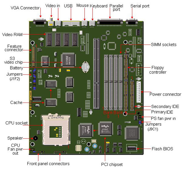
Uses the 321-pin Type 7 Zero Insertion Force (ZIF) CPU socket.
Supports the Pentium OverDrive Processor.
Not keyboard switchable.
Disable cache to slow down the system.
Uses 4/8/16/32 MB 72-pin simms, 60 or 70ns EDO (See below) or Fast Paged RAM up to a maximum of 128MB.Supports only non-parity DRAM.
1. Bank by bank support for EDO or Fast Page Mode DRAM with automatic presence detect for EDO DRAM. 60ns EDO required for 66 MHz bus speeds, and 70ns EDO required for 50 & 60 MHz bus speed. 70ns Fast Page Mode required for 50, 60, and 66 MHz bus speeds. EDO and Fast Page Mode can be mixed in separate banks.
2. Four 32 bit SIMM sockets 4 MB, 8 MB, 16 MB, 32 MB in either single or double sided configurations. Simms mustbe added in pairs. SIMM sockets can be populated in any order. ONE or more simms may be located under the peripheral bay in the Packard Bell "all-in-one" (Spectria) chassis.
3. Bank 0 will be populated as the default from the factory.
4. No configuration jumpers: BIOS detects memory size, and memory type (EDO or Fast Page Mode).
5. Memory voltage requirements: 5V.
The PB680 uses S3 Inc. Trio64V+ or S3 Virge 3D PCI Video Chipset.
S3 Trio64V+ motherboards have 1MB expandable to 2MB using two 256Kx16-50ns SOJ EDO DRAM chips.
S3 Virge 3D motherboards have 2MB Non Upgradable.
The video memory upgrade is inserted in sockets U2J1 and U3J1. Pin 1 is at the front right corner of the socket. To install the chip, insert it into the socket and push until the chip snaps into place.