Packard Bell 800/900 M/Board
There are two revisions of the PB800/900 motherboard.
Revision C
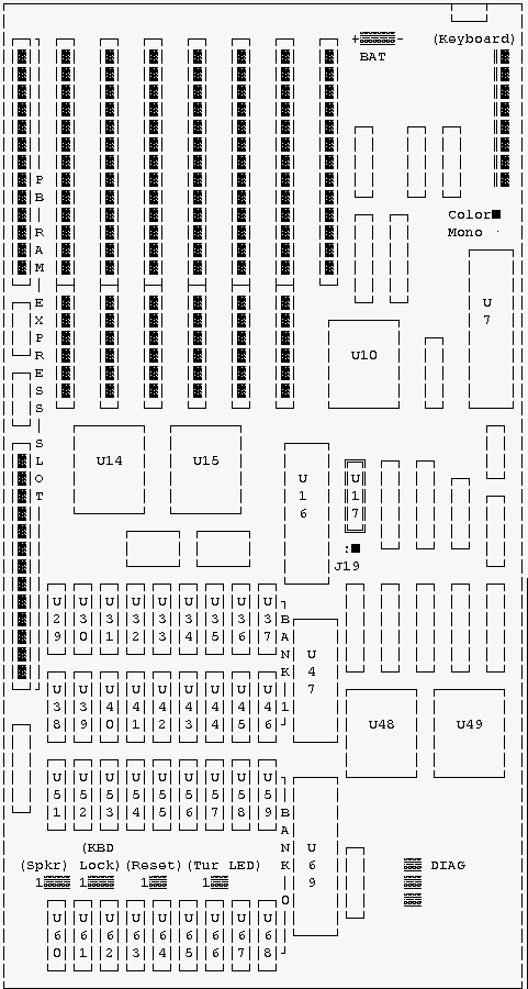
NOTE: Holds 1MB of RAM (256 x 1 chips), arranged in four rows of nine chips per row (8 bits of RAM and 1 parity bit.) The CMOS backup battery is a removable AT style battery.
Revision D
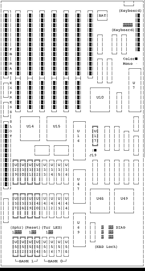
Holds 1MB of RAM (256K x 4 chips) arranged in 2 rows of 4 and parity 1 row of 4 (256K x 1 chips) upgradeable to 2MB with same chips plugged in adjacent sockets. CMOS Battery is soldered.
Specification
2 motherboard revisions: Rev.C requires matching BIOS and Chips chipsets. Supports 1MB. Rev.D supports 2MB on motherboard. There is no difference between the PB800 and the PB900.
- Battery : 3.6V DC NiCad
- BIOS : 2 X 32KB - Phoenix 3.10.14 BIOS. To access setup, Ctrl-Alt-S
- Cache : N/A
- Clock/Driver : (RTC)
- Cover Removal : 5 on back panel
- CPU : 80286-12 MHz, 80286-16 MHz. Keyboard Switches: (Ctrl)-(Alt)-(+) = 12/16 MHz, (Ctrl)-(Alt)-(-) = 8 MHz.
- Drive Cavities : 2 X 5 1/4" half (exposed). 1 X 5 1/4" half (enclosed)
- I/O Expansion slots : 6 x 16-bit ISA (5 open). 2 x 8-bit ISA (1 open)
- Interfaces :
- 1 DB-25 Parallel Port
- 1 RS-232, DB-9 Serial Port
- 1 RS232, DB-25 Serial Port
- 1 5-pin DIN Keyboard Port
- Power Supply : 145 watts, 110/220 v 50/60 Hz
- RAM : Standard on motherboard : 1 MB. Maximum on motherboard : Rev.c 1 MB
Rev.d 2 MB
- Speaker : Internal - cone on front
- Video : On expansion slot
Jumpers
| Jumper | Function | Pins | Description |
|---|
| J19 | 80287 Clock Speed | 1-2
3-4 | 80287-8
80287-10 |
| COLOUR/MONO | Display Mode | 1-2
2-3 | Colour
Monochrome |
Upgrades
- Cache Memory : This system does not support cache memory.
- Maths Co-Processor : This system will support an 80287-8 math coprocessor. It should be installed at location U16. Set J19 to pins 1-2. This system will also support an 80287-10 math co-processor. It should be installed at location U16. A 30-32MHz crystal need to be installed at U17. Set J19 to pins 2-3.
- RAM : Maximum on motherboard : Rev.c 1 MB Rev.d 2 MB. Use 256k chips, 100ns.
- Video Memory : This system has a video card installed. Replace the video card for video memory upgrades.